IODetect pcb update
Issues with previous design
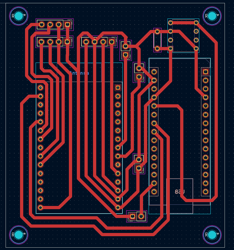
The main issue from the last print was that the pcb had signal traces that lied under and near the rf antenna of the eps32. The original plan was that this was not being used but it was later decided that the esp32 would be transmitting data using its 2.4GHz capabilities. I was aware that thius would be an issue as this could cause interfearance that would effect the signal integrity.
The previous design, which is inlcuded below, used a single layered design due to the contraints set by the pcb printer that we have access to. This constriant made me opt for a layout that routed under and near the antenna.
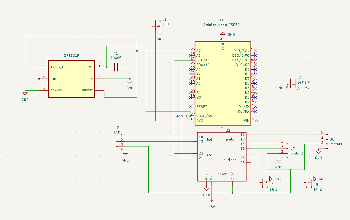
Another lkarge issue was that the measurements for the esp32 were off by around 1.5mm, specifically the distance between the pin rows. I ended up having to update the footprint in the changed pcb. We used third part esp32 which somehow had a varied size from the sizes that were stated on the espressif website. To fix thios the new measurements came directly from the esp32.
Main Change
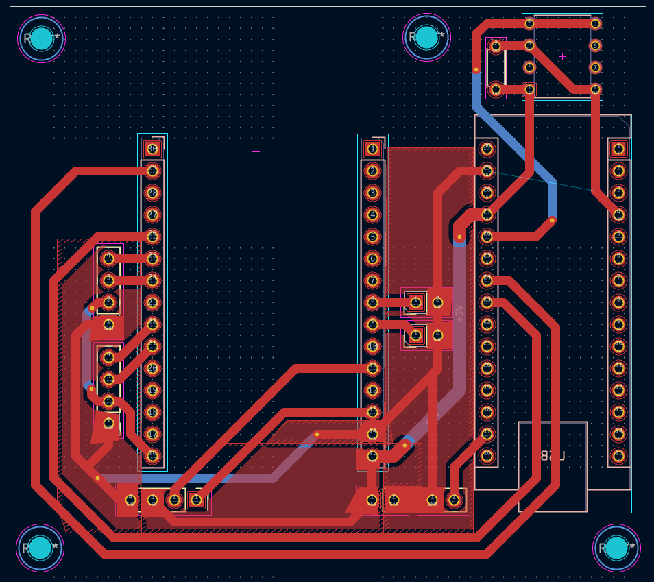
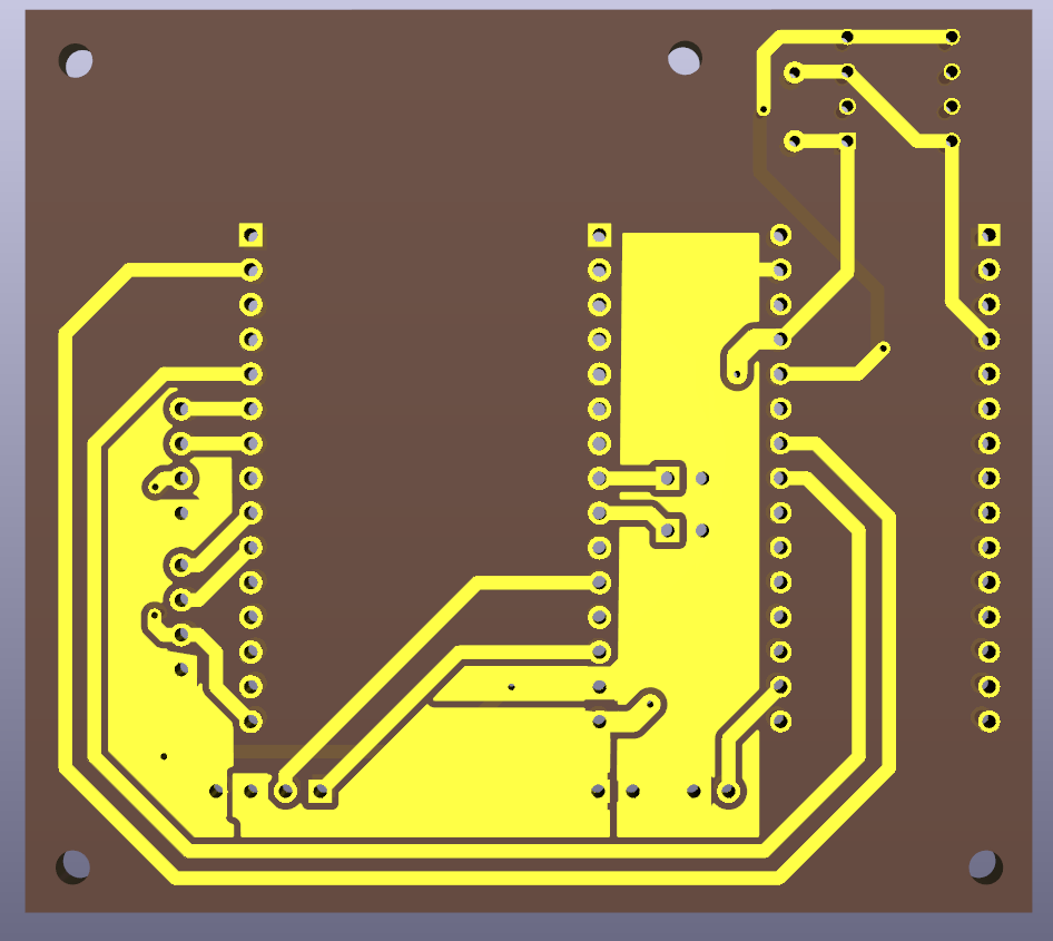
I ended up getting permisision from my team lead to update the design to use two layers. The new design has a larger size but now has no routing under the antenna.
The other main change I added was large copper pours for heat reduction. The coppper pours were added for ground and power planes specificcally in the higher current traces.
Upcoming Work
In the coming weeks we have to solder the components onto the board, and do testing on each individual components to ensure all the systems are working as intended. We also plan on fionalizing the pump system as well as the hardware code.