IODetect pcb
PCB Purpose
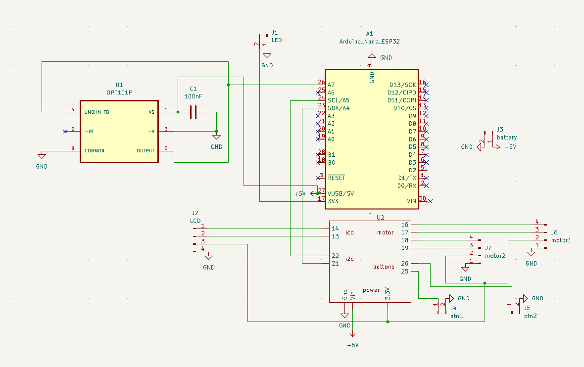
QBIT is working on a iodine deficiency detecting device that will use beer lamberts law to calculate iodine concentrations in pee. This is being done mainly using an opt101 sensor and a led of known wavelength. The project uses a esp32 for the main controller as well as an Arduino nano to collect samples from the opt sensor. The main purpose of the pcb is to allow all the peripherals to communicate with each other.
The board includes connections for analog to digital conversion of the opt sensor, power lines for all the electronics, 12c between the Arduino and esp, connections between the esp, motor shields, buttons and lcd display.
Constraints
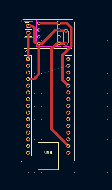
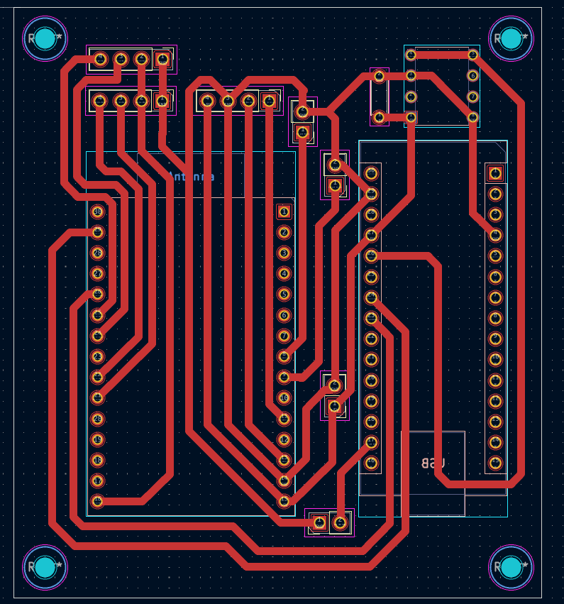
The main constraint when designing the pcb was the use of a pcb printer on campus. this made me rely on single layered boards. This honestly made design feel like a puzzle and ended up leading to a lot of head scratching and thinking. I ended up coming up with a solution, however it has one very large issue. I have traces running under the esp32 rf antenna, specifically digital lines which can cause interference with the antenna. I plan on making another version with 2 layers and getting permission to print it somehow to fix this issue.
The second constraint is size and form factor, the aim was to make the pcb as compact as possible to ensure that the final prototype would be portable and also that it would fit inside the casing that the physical team already designed. This was not much of an issue since the esp and Arduino didn’t take up much space.