Sound System Project
Disclaimer:
This project involves high-power electronics, including circuits that can carry dangerous voltages and currents. Improper design, construction, or handling may result in electric shock, burns, fire, equipment damage, or personal injury. The information shared here is for educational and documentation purposes and is not a complete guide. Therefore it should not be followed blindly. Stay safe.
One of my main points of interest in electrical engineering is audio engineering. I play a lot of guitar and have been building pedals for the past year. I decided that I wanted to put my analog design skills to the test by designing a sound system, with a focus on sound quality, range and power.
Research
The first step I took in starting this project was researching various topics that would provide valuable information. The first thing I researched was amplifiers. I quickly found that class D amplifiers would be best fitting for the high power usage of the sound system. I found that this article on analog.com by Eric Gaalaas was very helpful in understanding class D audio amplifiers. It also gives a lot of pretty helpful background on amplifiers themselves. Feel free to check it out. The main reason for my decision to use class D amplification was the high efficiency which would result in less heat dissipated as well as requiring less simple power systems. Another upside is that many class D amplifier ics don’t require a dual power supply (positive and negative rail) and instead only require a positive rail.
I also researched into speaker drivers (the part of a speaker that actually produces noise) as this would be the driving factor in the power supply design, amplifier ic choice, other circuitry and budget. Based on information from various forums, I decided to go with a 2.1 system. This is made of two stereo general drivers and one subwoofer. Many of the forum users pointed out that this was highly suitable for listening to music, which i figured would it’s main use. I decided to aim for 2x50W 4-8ohm stereo speakers with a 100W 4ohm subwoofer. This would cover the entire audible range while also providing enough volume.
As a side note for anyone wondering the ohm value is the impedance. Lower impedance allows higher power delivery from a given amplifier voltage, which can increase output capability. Many subwoofers are 2ohm to allow higher power transfer, especially in low-voltage systems like car audio. Another thing to keep in mind is that increasing power doesn’t relate to “loudness” of a speaker very much as human hearing is logarithmic. So you cant just double the power and expect twice the “loudness”.
While searching for drivers I was simultaneously looking at amplifier ics. I found Texas instruments’ TPA3116D2 and their TPA3221 which are affordable class D amps with very little distortion. They operate on 4.5 to 26V supply and 7 to 32V respectively. Both also have configurations to work with either a single mono output or 2 stereo outputs. Because of this they fit very well for my purpose. The difference between the 2 is that the 3116 outputs 100W mono and 2X50W stereo while the 3221 doubles this at 200W mono and 2X100W stereo. The 3221 mono configuration also safely supports 2ohm speakers. For these reasons I decided to go with the TPA3221.
I should state here that the watt values are max ratings. It is probably a good idea to operate at 70-80% of this in case of current spikes. Another thing, it is generally safe to operate a speaker that has higher impedance than that of what the amp is meant for. Ex. a 4ohm speaker can safely operate with a amp meant for 2ohm. Usually not the other way around, 2ohm speaker with 4ohm amp can cause over current and heat.
For this project I decided to implement a prebuilt power supply since they are cheap reliable and easy to get my hand on. The specifications for this are 24V output and 300W rating as dictated by my amp. This is a very generous power rating for safety purposes, but also leaves space for future upgrades. I could find power supply models that met these specs for around 30 CAD on amazon.
Systems
With the main components planned out I decided to plan out the systems that would be traversed from input to speaker.
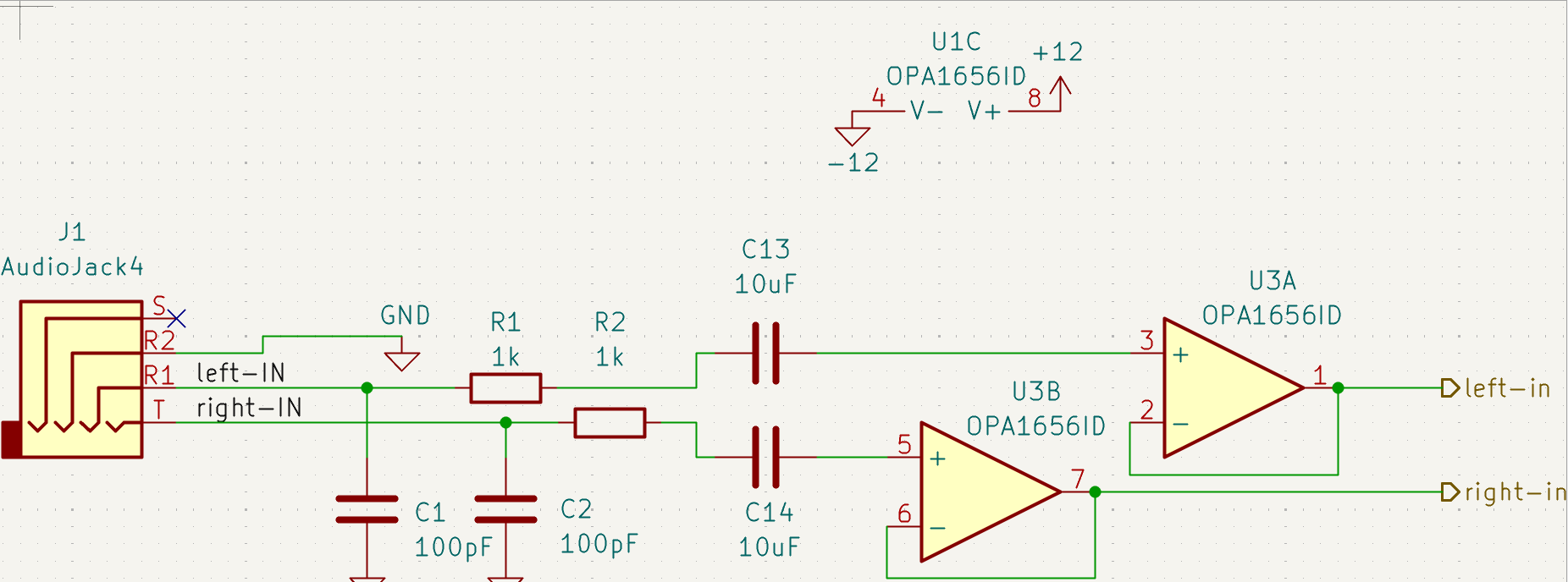
- Headphone jack input
- Buffer
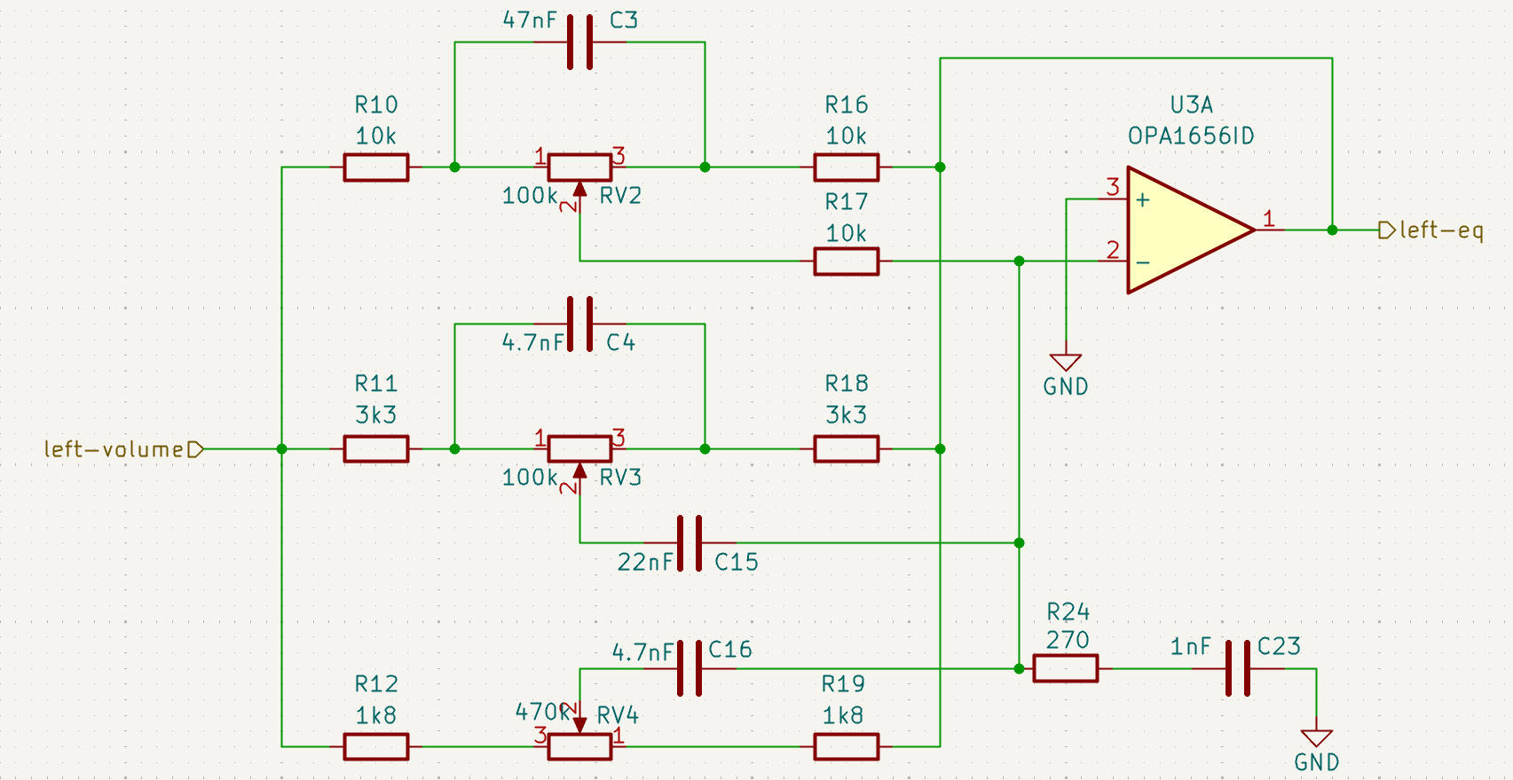
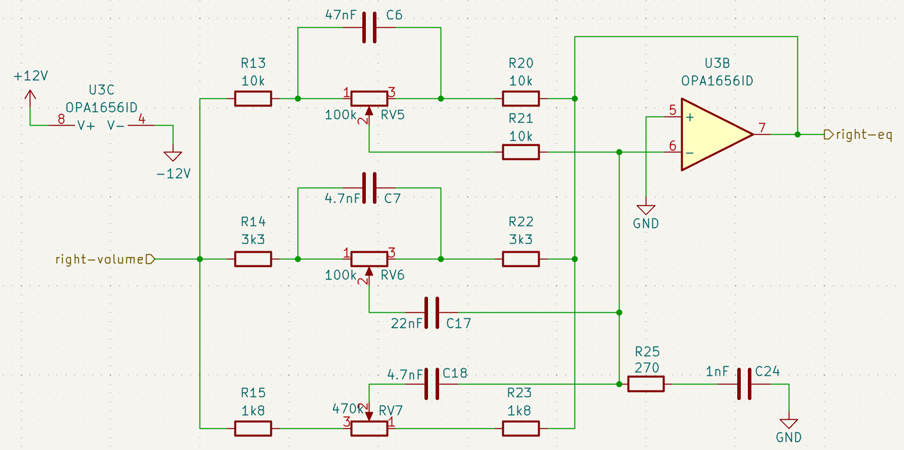
- 3 band equalizer
- Master volume
- Active crossover 2.1 split
- Amplifier
- Speaker output
Breakdown of 1-4
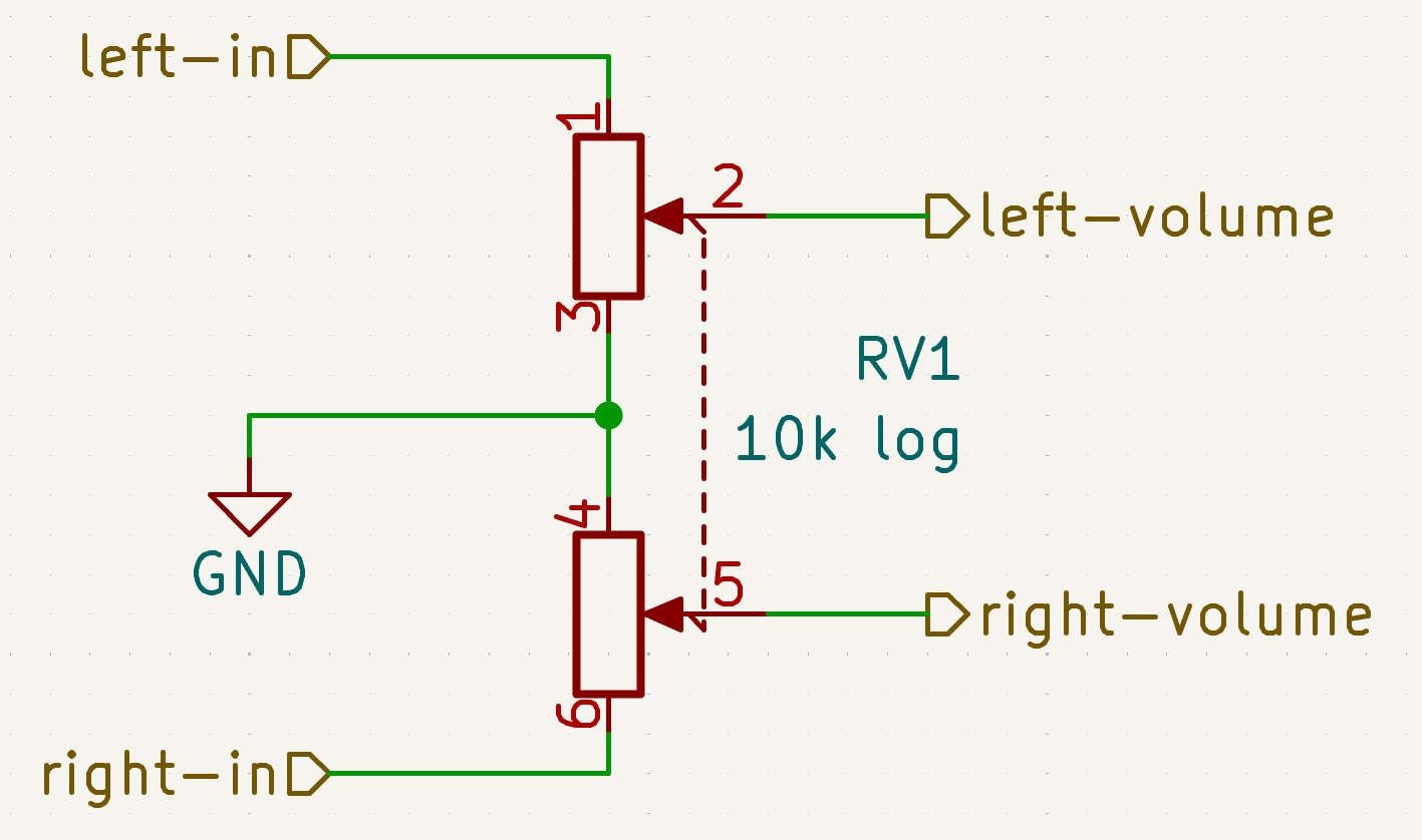
The input from the headphone jack is stereo, so the left and right lines will be kept isolated from each other. The input signal will be filtered to reduce noise and fed into an op amp based buffer (gain = 1) which will aim to minimize loading effects on the signal, that might be caused by the rest of the circuitry. Next the audio signals will be fed through a 3 band eq which will have a 3 potentiometer ui. After this a logarithmic potentiometer will be used as the master volume knob.
Breakdown of 5-7
An active crossover is used to split full-range audio into specific frequency bands (ex. highs, mids, and lows) directing them only to the drivers designed to handle them (tweeters, mid-ranges, woofers). This prevents damage to components, minimizes distortion, improves sound clarity, and increases overall efficiency. since I am using a 2.1 system I need a low pass filter for the subwoofer and 2 high pass filters for the 2 stereo speakers. After being split the audio signals are amplified with minimal distortion and output from the speakers.
It is also important to note that since the subwoofer is mono, the previously isolated right and left channels must be put together either using a summing amplifier or a resistive network before being fed into the amp.
Conclusion
With research completed I will soon begin design when I find time (I have 3 midterms coming up so might be a while). I expect to have to continue to research throughout the design process as there are many topics I am not very familiar with.
At this stage I have defined majority of the system: a Class D–based 2.1 system powered by a 24V supply, with buffering, equalization, and active crossover stages preceding amplification. While these choices are supported by research, the real validation will come during schematic design, simulation, PCB layout, and physical testing. This research serves as a technical foundation moving forward. The next step will be moving these concepts into detailed schematics and validating them through simulation before committing to hardware.
]]>